Diffusion and oxidation facility for fabrication of MOS transistors and integrated circuits
Equipment
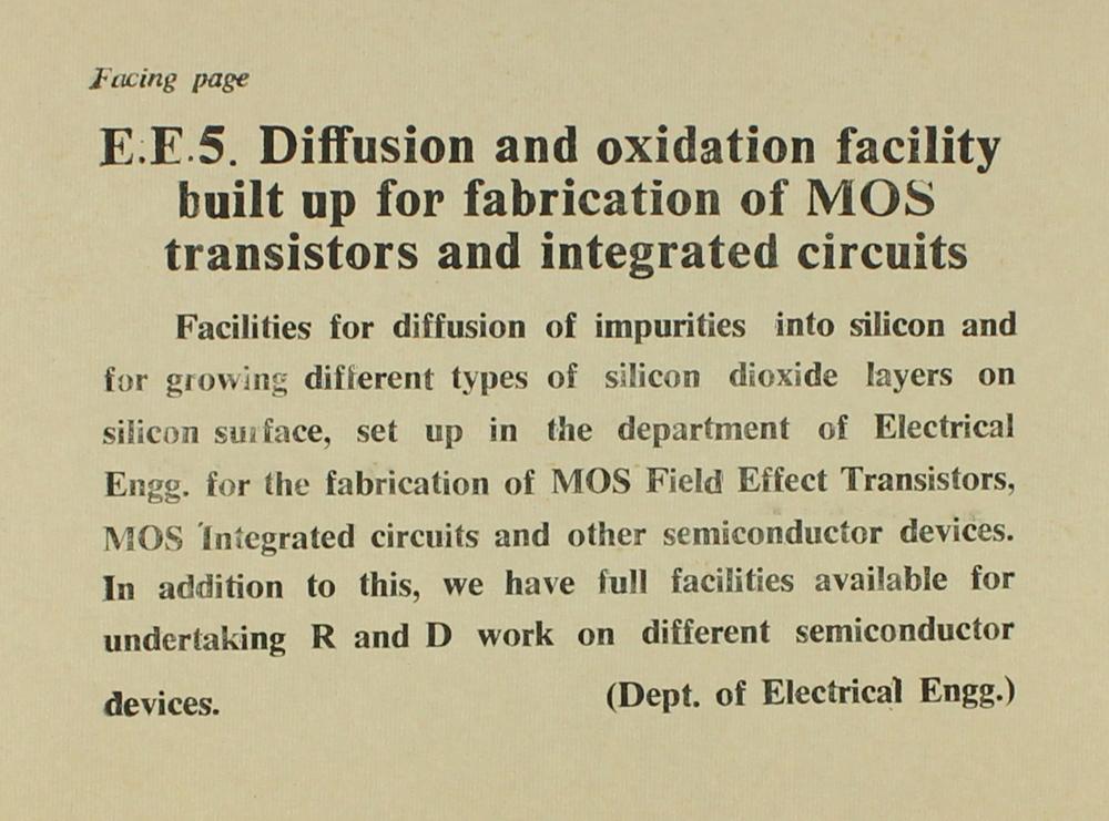
The image provides information on facilities for diffusion of impurities into silicon and for growing different types of silicon dioxide layers on silicon surfaces that was set up in the department of Electrical Engineering for the fabrication of MOS Field Effect Transistors, MOS Integrated circuits and other semiconductor devices. In addition to this, the image also states that the Department of Electrical Engineering has facilities available for undertaking R and D work on different semiconductor devices.


- Contribute
to the Centre -
 Monetary
Support  Digital
Material