Diffusion and oxidation facility for fabrication of MOS transistors and integrated circuits
Equipment
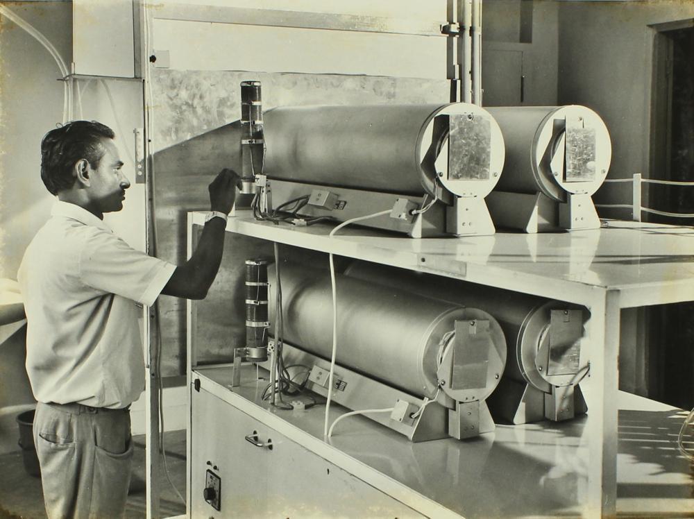
Seen in the image is a facility for diffusion of impurities into silicon and for growing different types of silicon dioxide layers on silicon surfaces that was set up in the department of Electrical Engineering for the fabrication of MOS Field Effect Transistors, MOS Integrated circuits and other semiconductor devices. The person in the image is yet to be identified.
A similar photograph can be found in album 0329: 001/0329/IMG_105825
Collection:
Central Photographic Section Collection
Album Name:
Photograph ID:
001/0040/IMG_1216_1
Album ID:
Date:
January 1976
Share:


- Contribute
to the Centre -
 Monetary
Support  Digital
Material